Scheme. Computer power supply Connecting the power supply at 200w
Read also
» Harmful recipes
» High voltage
» Generators
" Games
» Measurements
» Tools and technologies
» Interfaces
» Computers and peripherals
» Laser
" The medicine
» Monitors
" Music
» Beginners
» Open MK platforms
» Promising technologies
" Printed circuit boards
" Food
» Application of microcontrollers
» Radio
" Radio controlled models
» Retro
» Robotics
» CAD and software
» Lighting
» Networks
» Power electronics
» Solar energy
" Cellular
» Satellite equipment
" TV
" Telephone
» Theory
» Instructions for use
» Digital
» Arduino
Search by: " 200w switching power supply"
Added words from the dictionary: " power powerful power power food"
Box with the required number of sockets. Diodes D1 to 6 listed in the parts list can be used if power load connected to the main socket does not exceed 500 W. For a load of 800 1000 W, you need to take diodes ...
control socket. Use BY550-800 diodes for up to 800 - 1000W. For less demanding appliances, 1N4007 diodes will allow up to 200W power. The Triac type suggested in the Parts List for D7 will allow a total power available to the Switched ...
.. a PC, a Monitor and a Printer could be connected to the Switched Sockets and will be running after the lamp is switched on. Switching off the lamp, all the above mentioned appliances will be automatically switched off. A further...
..appliances will be automatically switched off. A further application is the control of a High Fidelity chain, plugging the power Amplifier in the Control Socket and - for example - CD Player, Tape Recorder, and Tuner in the Switched ...
.. if the control appliance is on or off. This could also happen when devices connected to the mains by means of plug-in power supply adapters are used as control appliances, due to their lack of a mains switch. In spite of this restriction, ...
20-07-2009
20-09-2012
Hello! In general, such a story happened. They brought me a burnt PSU SWITCHING POWER SUPPLY MODEL: LC-235ATX. I ask what happened to him. And they started telling me. Decided...
.. sravnitj s lampockoi 12V/21W tem bolee esli ona escio i podkliucena k +5V..! I read on some site that you can increase power PSU replacement of input capacitors, diode bridge, high-voltage transistors, etc. But the power...
.. and from this develop the question. Most likely, you will not be able to find the exact circuit for your PSU. Some diagrams are posted in the section FOOD-> Charger based on a computer PSU. There are a whole bunch of books on the principles of operation of computer power supplies. Here's one of...
02-05-2006
LTC4412) drives two p-channel MOSFETs that act as a near-ideal diode by switching food circuits from an AC voltage source to a battery, and vice versa. Voltage drop across MOSFET...
Rectified voltage drops below the battery voltage, the battery takes over to provide LED power. The circuit has some small switching losses, which should be acceptable as long as IC2, a 12 V PB137 battery-charging circuit from ...
.. Yu, Juno Lighting Group, Des Plaines, IL; Edited by Martin Rowe and Fran Granville Power three to six LEDs from an ac- or dc- power source and charge a backup battery. LEDs find wide use in emergency ...
.. or two capacitors filter into dc. The battery (not shown) is a 12 V lead-acid type. IC1 compares the battery voltage to the supply voltage. When the rectified voltage drops below the battery voltage, the battery takes over to provide LED ...
03-08-2010
The case can not be used in the circuit voltage regulator U2. This solution has its advantages. it is possible to connect more powerful cooling Fan. If your power supply does not have a +12 V output, then this connector must be left ...
.. using a shunt that is connected in series with the load in the circuit of the negative (common) terminal of the power supply. Food the device receives from the main power supply (i.e. from the power supply that you are upgrading). ...
That pin should be connected even if +12V DC is connected to J2 pin. Voltage from that pin deliver information for fan switching. J4 - Measuring signal connector. Multimeter is suitable for voltage and current measurement in PSU, ...
.. function of the multimeter is that it can control (switch on and off) an electric fan used to cool the main heatsink. The power threshold at which the fan switches on can be adjusted using One Touch Button Setup. Specifications-...
.. where the current sense shunt resistor is connected in series with load at the negative voltage rail. It needs only one supply voltage that can be acquired from main PSU. An additional function of the multimeter is that it can control ...
13-08-2010
This typical power supply uses the LM2674 chip from National Semiconductor, which has been manufacturing and designing components for switching converters for many years. Instead of LM2674, you can use the LM2671 chip. ...
Voltage. Within the specified application, the supplies can deliver currents of up to 500 mA. Note-worthy is the high switching frequency of 260 kHz. This has the advantage that only low-value inductors and capacitors are needed, ...
..Switch Mode power Supply circuit use the IC from National Semiconductor has been producing and designing ICs for use in ...
06-01-2011
RADIOLOTSMAN, August 2014 Jim Drew, Linear Technology LT Journal food quite often required in analog circuits to create a virtual ground at the outputs of amplifiers. How...
Up and the cycle repeats. This hysteretic method of providing a regulated output reduces losses associated with MOSFETs switching and maintains an output voltage at light loads. The buck regulator is able to support 50 mA of average ...
.. Drew, Linear Technology LT Journal Analog circuits often need a split-voltage power supply to achieve a virtual ground at the output of an amplifier. These split voltages power supplies are ...
The best scheme of a standard ATX PSU
ATX POWER SUPPLY DTK PTP-2038 200W
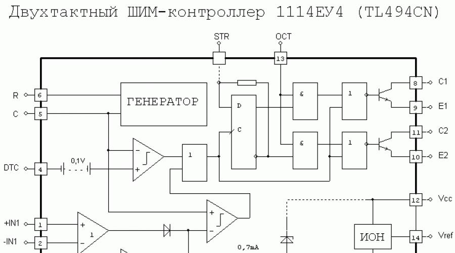
TL494
Peculiarities:
- Full range of PWM control functions
- Output sinking or sinking current of each output 200mA
- Can be operated in two-stroke or single-stroke mode
- Built-in double-pulse suppression circuit
- Wide adjustment range
- Output reference voltage 5V + -05%
- Simply Organized Synchronization
general description:
Designed specifically for building TTIs, the TL493/4/5 ICs provide the designer with advanced options when designing TTI control circuits. The TL493/4/5 includes an error amplifier, a built-in variable oscillator, a dead time adjustment comparator, a control trigger, a 5V precision reference, and an output stage control circuit. The error amplifier provides a common mode voltage ranging from -0.3…(Vcc-2) V. The dead time control comparator has a constant offset that limits the minimum dead time to about 5%.
It is allowed to synchronize the built-in generator by connecting the output R to the output of the reference voltage and supplying the input sawtooth voltage to the output C, which is used in the synchronous operation of several IVP circuits.
Independent output drivers on transistors provide the ability to operate the output stage according to a common emitter circuit or an emitter follower circuit. The output stage of the TL493 / 4/5 microcircuits operates in single-cycle or push-pull mode with the ability to select the mode using a special input. Built-in circuitry monitors each output and disables double pulse output in push-pull mode.
Devices with the suffix L guarantee normal operation in the temperature range -5...85C, with the suffix C guarantee normal operation in the temperature range 0...70C.
Structural scheme:

Hull pinout:

Parameter limits:
Supply voltage…………………………………………………………….41V
Amplifier input voltage………………………………………...(Vcc+0.3)V
Collector output voltage…………………………………………...…41V
Collector output current………………………………………………….…250mA
Total power dissipation in continuous mode……………………….1W
Operating ambient temperature range:
With suffix L…………………………………………………………………-25..85C
With suffix С…………………………………………………………………..0..70С
Storage temperature range ………………………………………..-65…+150C
The power supply is the most important part of any device, especially when it comes to a computer power supply. At one time I was engaged in their repair, so some schemes have accumulated that can help you figure it out and, if necessary, repair them.
To begin with, a small educational program on BP:
The PSU for a computer is built on the basis of a push-pull converter with a transformerless input. It is safe to say that 95 percent of all power supplies for computers are built on this principle. The output voltage generation cycle contains several steps: the input voltage is rectified, smoothed and fed to the power switches of the push-pull converter. The work of these keys is carried out by a specialized microcircuit, usually called a PWM controller. This controller generates pulses applied to power elements, usually power bipolar transistors, but recently there has been interest in powerful field-effect transistors, so they can also be found in power supplies. Since the conversion circuit is push-pull, we have two transistors that must switch alternately with each other, if they turn on at the same time, then we can safely assume that the PSU is ready for repair - in this case, the power elements burn out, sometimes the pulse transformer can burn out and more something to load. The task of the controller is to ensure that such a situation does not occur in principle, it also monitors the output voltage, usually this is a + 5V supply circuit, i.e. this voltage is used for the feedback circuit and all other voltages are stabilized through it. By the way, in Chinese PSUs, additional stabilization along the + 12V, -12V, + 3.3V circuits is not provided.
Voltage regulation is carried out according to the pulse-width method: the duty cycle of the pulse usually changes, i.e. log width. 1 to the width of the entire pulse. The more log.1, the higher the output voltage. All this can be found in the special literature on power rectifier technology.
After the keys, there is a pulse transformer, which transfers energy from the primary circuit to the secondary and at the same time provides galvanic isolation from the 220V power circuit. Further, an alternating voltage is removed from the secondary windings, which is rectified, smoothed and fed to the output to power the motherboard and all computer components. This is a general description that is not without flaws. For questions about power electronics, it is worth turning to specialized textbooks and resources.
Below is the wiring diagram for AT and ATX power supplies:
| AT | ATX | ||||||||||||||||||||||||||||||||||||||||||||
|
|||||||||||||||||||||||||||||||||||||||||||||
To start the ATX power supply, connect the Power Supply On wire to ground (black wire). The following are power supply diagrams for a computer:
ATX power supplies:
| № |
File |
Description |
|---|---|---|
| 1 |
An ATX power supply circuit based on the TL494 chip is presented. | |
| 2 |
ATX POWER SUPPLY DTK PTP-2038 200W. | |
| 3 |
I needed a lightweight power supply, for different things (expeditions, power supply of various HF and VHF receivers or in order not to carry a transformer power supply with you when moving to another apartment). After reading the available information on the network about the alteration of computer power supplies, I realized that I would have to figure it out myself. Everything I found was described somehow chaotically and not entirely clear (for me). Here I will tell you, in order, how I redid several different blocks. The differences will be described separately. So, I found some PSUs from old PC386 200W (at least that's what it says on the cover). Usually on the cases of such PSUs they write something like this: +5V/20A , -5V/500mA , +12V/8A , -12V/500mA The currents indicated on the +5 and +12V buses are pulsed. It is impossible to constantly load the PSU with such currents, high-voltage transistors will overheat and crack. Subtract 25% from the maximum pulse current and get the current that the PSU can keep constantly, in this case it is 10A and up to 14-16A for a short time (no more than 20sec). Actually, here it is necessary to clarify that 200W PSUs are different, of those that I came across, not everyone could hold 20A even for a short time! Many pulled only 15A, and some up to 10A. Keep that in mind!

I want to note that a specific PSU model does not play a role, since they are all made almost according to the same scheme with slight variations. The most critical point is the presence of the DBL494 chip or its analogues. I came across PSU with one chip 494 and with two chips 7500 and 339. Everything else does not matter much. If you have the opportunity to choose a PSU from several, first of all, pay attention to the size of the pulse transformer (the bigger, the better) and the presence of a network filter. It’s good when the surge protector is already soldered, otherwise you will have to unsolder it yourself in order to reduce interference. It's easy, wind 10 turns on a firrite ring and put two capacitors, places for these parts are already provided on the board.
PRIORITY MODIFICATIONS
To begin with, let's do a few simple things, after which you will get a well-functioning power supply with an output voltage of 13.8V, a constant current of up to 4 - 8A and a short-term current of up to 12A. You make sure that the PSU is working and decide whether you needcontinue modifications.
1. We disassemble the power supply and pull the board out of the case and carefully clean it with a brush and a vacuum cleaner. There should be no dust. After that, we solder all the bundles of wires going to the +12, -12, +5 and -5V buses.
2.
you need to find (on board) chip DBL494 (in other boards it costs 7500, this is an analogue), switch the protection priority from the + 5V bus to + 12V and set the voltage we need (13 - 14V).
Two resistors depart from the 1st leg of the DBL494 chip (sometimes more, but it doesn't matter), one goes to the body, the other to the + 5V bus. We need him, carefully solder one of his legs (break connection).
3.
Now, between the + 12V bus and the first DBL494 foot microcircuit, we solder a resistor 18 - 33k. You can put a trimmer, set the voltage to + 14V and then replace it with a constant one. I recommend setting it to 14.0V rather than 13.8V, because most branded HF-VHF equipment works best at this voltage.

SETUP AND ADJUSTMENT
1. It's time to turn on our PSU to check if we did everything right. The fan can not be connected and the board itself can not be inserted into the case. We turn on the PSU, without load, connect a voltmeter to the + 12V bus and see what voltage it is. With a trimming resistor, which stands between the first leg of the DBL494 chip and the + 12V bus, we set the voltage from 13.9 to + 14.0V.
2. Now check the voltage between the first and seventh legs of the DBL494 chip, it should be at least 2V and not more than 3V. If this is not the case, select a resistor between the first leg and the body and the first leg and the +12V rail. Pay special attention to this point, this is the key point. If the voltage is higher or lower than the specified one, the power supply will work worse, be unstable, and keep a smaller load.
3. Short the +12V bus to the case with a thin wire, the voltage must disappear in order for it to recover - turn off the PSU for a couple of minutes (need to empty the tanks) and turn it on again. Has there been tension? Good! As you can see, the protection works. What didn't work?! Then we throw out this PSU, it does not suit us and take another ... hee.
So, the first stage can be considered completed. Insert the board into the case, bring out the terminals for connecting the radio station. You can use the power supply! Connect the transceiver, but it is not yet possible to give a load of more than 12A! Vehicle VHF station, will operate at full power (50W), and in the HF transceiver you will have to install 40-60% of the power. What happens if you load the PSU with a large current? It's okay, protection usually works and the output voltage disappears. If the protection does not work, the high-voltage transistors will overheat and burst. In this case, the voltage will simply disappear and there will be no consequences for the equipment. After replacing them, the PSU is working again!
1. We turn the fan on the contrary, it should blow inside the case. We put washers under two screws of the fan to turn it around a little, otherwise it blows only on high-voltage transistors, this is wrong, it is necessary that the air flow be directed both to the diode assemblies and to the ferrite ring.
Before this, it is advisable to lubricate the fan. If it makes a lot of noise, put a 60 - 150 ohm 2W resistor in series with it. or make a rotation regulator depending on the heating of the radiators, but more on that below.
2.
Remove two terminals from the PSU to connect the transceiver. From the 12V bus to the terminal, run 5 wires from the bundle that you soldered at the beginning. Between terminalsput a non-polar capacitor at 1uF and an LED with a resistor. Negative wire, also bring to the terminal with five wires. In some power supplies, in parallel with the terminals to which the transceiver is connected, put a resistor with a resistance of 300 - 560 ohms. This is a load so that the protection does not work. The output circuit should look something like the one shown in the diagram.


two radiators, a pulse transformer, a choke on a ferrite ring, a choke on a ferrite rod. Now our task is to reduce heat transfer and increase the maximum load current. As I said earlier, it can go up to 16A (for 200W PSU).
4.
Solder the choke on the ferrite rod from the + 5V bus and put it on the + 12V bus, the choke standing there earlier (it is taller and wound with a thin wire) solder and discard. Now the throttle will practically not heat up or will, but not so much. There are simply no chokes on some boards, you can do without it, but it is desirable that it be for better filtering of possible interference.

5. A choke is wound on a large ferrite ring to filter out impulse noise. The + 12V bus on it is wound with a thinner wire, and the + 5V bus is the thickest. Solder this ring carefully and swap the windings for the + 12V and + 5V buses (or turn on all windings in parallel). Now the + 12V bus passes through this inductor, with the thickest wire. As a result, this inductor will heat up much less.
6. The PSU has two radiators, one for high-power high-voltage transistors, the other for +5 and +12V diode assemblies. I came across several varieties of radiators. If, in your PSU, the dimensions of both radiators are 55x53x2mm and they have ribs in the upper part (as in the photo) - you can count on 15A. When the radiators are smaller, it is not recommended to load the PSU with a current of more than 10A. When the radiators are thicker and have an additional pad at the top, you are lucky, this is the best option, you can get 20A within a minute. If the heatsinks are small, to improve heat dissipation, you can attach a small plate of duralumin or a half from the heatsink of an old processor to them. Pay attention to whether the high-voltage transitors are well screwed to the radiator, sometimes they hang out.
7. We solder the electrolytic capacitors on the + 12V bus, put 4700x25V in their place. It is advisable to remove the capacitors on the + 5V bus, just so that there is more free space and the air from the fan blows the parts better.


8. On the board you see two high voltage electrolytes, usually 220x200V. Replace them with two 680x350V, in extreme cases, connect in parallel two of 220+220=440mKf. This is important and the point here is not only filtering, impulse noise will be weakened and resistance to maximum loads will increase. The result can be viewed with an oscilloscope. In general, you must do it!
9. It is desirable that the fan changes speed depending on the heating of the PSU and does not spin when there is no load. This will extend the life of the fan and reduce noise. I offer two simple and reliable schemes. If you have a thermistor, look at the circuit in the middle, set the temperature of the thermistor response to about + 40C with a trimmer resistor. Transistor, you need to install exactly KT503 with maximum current gain (it is important), other types of transistors perform worse. Any type of NTC thermistor, this means that when heated, its resistance should decrease. You can use a thermistor with a different rating. The tuning resistor should be multi-turn, so it is easier and more accurate to adjust the temperature of the fan operation. We fasten the board with the circuit to the free ear of the fan. We attach the thermistor to the throttle on the ferrite ring, it heats up faster and stronger than other parts. You can glue the thermistor to the 12V diode assembly. It is important that none of the thermistor leads short to the radiator!!! In some PSUs, there are fans with a high current consumption, in this case, after KT503, you need to put KT815.
Here is a complete description of the circuit diagram for one of the 200-watt switching power supplies (PS6220C, made in Taiwan).

The alternating mains voltage is supplied through the PWR SW mains switch through the F101 4A mains fuse, noise suppression filters formed by elements C101, R101, L101, C104, C103, C102 and chokes L102, L103 to:
- output three-pin connector, to which the display power cable can be docked;
- two-pin connector JP1, the counterpart of which is located on the board.
From the JP1 connector, the AC mains voltage is supplied to:
- bridge rectification circuit VR1 through the thermistor THR1;
- the primary winding of the starting transformer T1.
At the output of the rectifier VR1, the smoothing capacitances of the filter C1, C2 are turned on. The THR thermistor limits the initial inrush charging current of these capacitors. The 115V/230V switch SW enables the UPS to be powered both from the 220-240V network and from the 110/127V network.
High-ohmic resistors R1, R2, shunt capacitors C1, C2 are baluns (equalize the voltages on C1 and C2), and also ensure the discharge of these capacitors after the UPS is turned off from the mains. The result of the operation of the input circuits is the appearance on the bus of the rectified voltage of the DC network Uep, equal to +310 V, with some ripples. This UPS uses a start-up circuit with forced (external) excitation, which is implemented on a special starting transformer T1, on the secondary winding of which, after the UPS is connected to the network, an alternating voltage appears with the frequency of the supply network. This voltage is rectified by diodes D25, D26, which form with the secondary winding T1 a full-wave rectification circuit with a midpoint. C30 is the smoothing capacitance of the filter, on which a constant voltage is generated, which is used to power the control chip U4.
The TL494 IC is traditionally used as a control chip in this UPS.
The supply voltage from the capacitor C30 is applied to terminal 12 U4. As a result, the output voltage of the internal reference source Uref = -5 V appears at pin 14 of U4, the internal sawtooth voltage generator of the microcircuit starts, and control voltages appear at pins 8 and 11, which are sequences of rectangular pulses with negative leading edges, shifted relative to each other for half a period. Elements C29, R50, connected to pins 5 and 6 of the U4 chip, determine the frequency of the sawtooth voltage generated by the internal chip generator.
The matching stage in this UPS is made according to a transistorless circuit with separate control. The supply voltage from the capacitor C30 is supplied to the midpoints of the primary windings of the control transformers T2, T3. The output transistors of the IC U4 perform the functions of the matching stage transistors and are connected according to the OE circuit. The emitters of both transistors (pins 9 and 10 of the microcircuit) are connected to the "body". The collector loads of these transistors are the primary half-windings of the control transformers T2, T3, connected to terminals 8, 11 of the U4 microcircuit (open collectors of the output transistors). The other halves of the primary windings T2, T3 with diodes D22, D23 connected to them form the demagnetization circuits of the cores of these transformers.
Transformers T2, T3 control the powerful transistors of the half-bridge inverter.
Switching the output transistors of the microcircuit cause the appearance of pulsed control EMF on the secondary windings of the control transformers T2, T3. Under the influence of these EMF power transistors Q1, Q2 alternately open with adjustable pauses ("dead zones"). Therefore, an alternating current flows through the primary winding of the power pulse transformer T5 in the form of sawtooth current pulses. This is due to the fact that the primary winding T5 is included in the diagonal of the electric bridge, one arm of which is formed by transistors Q1, Q2, and the other by capacitors C1, C2. Therefore, when opening any of the transistors Q1, Q2, the primary winding T5 is connected to one of the capacitors C1 or C2, which causes the current to flow through it during the entire time the transistor is open.
Damper diodes D1, D2 return the energy stored in the leakage inductance of the primary winding T5 during the closed state of transistors Q1, Q2 back to the source (recuperation).
Capacitor C3, connected in series with the primary winding T5, eliminates the DC component of the current through the primary winding T5, thereby eliminating undesirable bias of its core.
Resistors R3, R4 and R5, R6 form the base dividers for power transistors Q1, Q2, respectively, and provide the optimal switching mode in terms of dynamic power losses on these transistors.
The flow of alternating current through the primary winding T5 causes the presence of alternating rectangular pulse EMF on the secondary windings of this transformer.
The power transformer T5 has three secondary windings, each of which has a lead from the midpoint.
Winding IV provides an output voltage of +5 V. Diode assembly SD2 (half-bridge) forms with winding IV a full-wave rectification circuit with a midpoint (the midpoint of winding IV is grounded).
Diodes assembly SD2 are diodes with a Schottky barrier, which achieves the required speed and increases the efficiency of the rectifier.
Winding III together with winding IV provides an output voltage of +12 V together with the diode assembly (half-bridge) SD1. This assembly forms with winding III a full-wave rectification circuit with a midpoint. However, the middle point of winding III is not grounded, but connected to the +5 V output voltage bus. This will make it possible to use Schottky diodes in the +12 V output channel, since the reverse voltage applied to the rectifier diodes during this connection decreases to a level acceptable for Schottky diodes.
Elements L1, C6, C7 form a smoothing filter in the +12 V channel.
Resistors R9, R12 are designed to accelerate the discharge of the output capacitors of the +5 V and +12 V buses after the UPS is turned off from the mains.
Winding II with five taps provides -5 V and -12 V negative output voltages.
Two discrete diodes D3, D4 form a full-wave rectification half-bridge in the -12 V output channel, and diodes D5, D6 - in the -5 V channel.
Elements L3, C14 and L2, C12 form smoothing filters for these channels.
Winding II, as well as winding III, is shunted by a soothing RC circuit R13, C13.
The center point of winding II is grounded.
Stabilization of output voltages is carried out in different ways in different channels.
Negative output voltages -5 V and -12 V are stabilized using linear integrated three-terminal stabilizers U4 (type 7905) and U2 (type 7912).
To do this, the output voltages of the rectifiers from the capacitors C14, C15 are supplied to the inputs of these stabilizers. On the output capacitors C16, C17, stabilized output voltages of -12 V and -5 V are obtained.
Diodes D7, D9 provide discharge of the output capacitors C16, C17 through resistors R14, R15 after the UPS is turned off from the network. Otherwise, these capacitors would be discharged through the stabilizer circuit, which is undesirable.
Through resistors R14, R15, capacitors C14, C15 are also discharged.
Diodes D5, D10 perform a protective function in the event of a breakdown of the rectifier diodes.
If at least one of these diodes (D3, D4, D5 or D6) turns out to be "broken", then in the absence of diodes D5, D10, a positive pulse voltage would be applied to the input of the integral stabilizer U1 (or U2), and through electrolytic capacitors C14 or C15 an alternating current would flow, which would lead to their failure.
The presence of diodes D5, D10 in this case eliminates the possibility of such a situation, because current flows through them.
For example, if the diode D3 is "broken", the positive part of the period when D3 must be closed, the current will close in the circuit: to-and D3 - L3 D7-D5- "case".
Stabilization of the output voltage +5 V is carried out by the PWM method. To do this, a measuring resistive divider R51, R52 is connected to the +5 V output voltage bus. A signal proportional to the output voltage level in the +5 V channel is taken from the resistor R51 and fed to the inverting input of the error amplifier DA3 (pin 1 of the control chip). The direct input of this amplifier (pin 2) is supplied with a reference voltage level, taken from the resistor R48, which is included in the divider VR1, R49, R48, which is connected to the output of the internal reference source of the U4 microcircuit Uref = +5 V. When the voltage level on the bus + 5 V under the influence of various destabilizing factors, there is a change in the magnitude of the mismatch (error) between the reference and controlled voltage levels at the inputs of the error amplifier DA3. As a result, the width (duration) of the control pulses at pins 8 and 11 of the U4 chip changes in such a way as to return the deviated +5 V output voltage to the nominal value (when the voltage on the +5 V bus decreases, the width of the control pulses increases, and when this voltage increases - decreases).
The output voltage +12 V in this UPS is not stabilized.
The output voltage level in this UPS is adjusted only for the +5 V and +12 V channels. This adjustment is carried out by changing the reference voltage level at the direct input of the error amplifier DA3 using the trimmer resistor VR1.
When the position of the VR1 slider is changed during the UPS configuration, the voltage level on the +5 V bus will change within certain limits, and hence on the +12 V bus, because voltage from the +5 V bus is supplied to the middle point of the winding III.
The combined protection of this UPS includes:
- a limiting circuit for controlling the width of the control pulses;
- an incomplete output overvoltage control circuit (only on the +5 V bus).
Let's look at each of these schemes.
The limiting control circuit uses a T4 current transformer as a sensor, the primary winding of which is connected in series with the primary winding of the T5 power pulse transformer.
Resistor R42 is the load of the secondary winding T4, and diodes D20, D21 form a full-wave circuit for rectifying the alternating pulse voltage taken from the load R42.
Resistors R59, R51 form a divider. Part of the voltage is smoothed by capacitor C25. The voltage level on this capacitor proportionally depends on the width of the control pulses at the bases of power transistors Q1, Q2. This level is fed through the resistor R44 to the inverting input of the error amplifier DA4 (pin 15 of the U4 chip). The direct input of this amplifier (pin 16) is grounded. Diodes D20, D21 are connected so that the capacitor C25, when current flows through these diodes, is charged to a negative (relative to the common wire) voltage.
In normal operation, when the width of the control pulses does not go beyond the allowable limits, the potential of pin 15 is positive, due to the connection of this pin through the resistor R45 with the Uref bus. If the control pulse width is increased excessively for any reason, the negative voltage across the capacitor C25 increases, and the potential of output 15 becomes negative. This leads to the output voltage of the error amplifier DA4, which was previously equal to 0 V. A further increase in the width of the control pulses leads to the fact that the switching control of the PWM comparator DA2 is transferred to the amplifier DA4, and the subsequent increase in the width of the control pulses no longer occurs (restricted mode), as the width of these pulses ceases to depend on the level of the feedback signal at the direct input of the error amplifier DA3.
The protection circuit against short circuit in loads can be conditionally divided into protection of channels for generating positive voltages and protection of channels for generating negative voltages, which are implemented in circuitry in approximately the same way.
The sensor of the short circuit protection circuit in the loads of the channels for generating positive voltages (+5 V and +12 V) is a diode-resistive divider D11, R17, connected between the output buses of these channels. The voltage level at the anode of diode D11 is a controlled signal. In normal operation, when the voltages on the output buses of the +5 V and +12 V channels have nominal values, the anode potential of the diode D11 is about +5.8 V, because through the divider-sensor, current flows from the +12 V bus to the +5 V bus along the circuit: +12 V bus - R17-D11 - +5 V bus.
The controlled signal from the anode D11 is fed to the resistive divider R18, R19. Part of this voltage is taken from the resistor R19 and fed to the direct input of the comparator 1 of the U3 chip of the LM339N type. The reference voltage level is supplied to the inverting input of this comparator from the resistor R27 of the divider R26, R27 connected to the output of the reference source Uref=+5 V of the control chip U4. The reference level is chosen such that, during normal operation, the potential of the direct input of comparator 1 would exceed the potential of the inverse input. Then the output transistor of comparator 1 is closed, and the UPS circuit functions normally in PWM mode.
In the event of a short circuit in the load of the +12 V channel, for example, the anode potential of the diode D11 becomes equal to 0 V, so the potential of the inverting input of comparator 1 will become higher than the potential of the direct input, and the output transistor of the comparator will turn on. This will cause the Q4 transistor to close, which is normally open by the base current flowing through the circuit: Upom bus - R39 - R36 b-e Q4 - "body".
Turning on the output transistor of comparator 1 connects resistor R39 to the "body", and therefore transistor Q4 is passively closed by zero bias. Closing the transistor Q4 entails the charging of the capacitor C22, which acts as a protection delay link. The delay is necessary for those reasons that in the process of the UPS entering the mode, the output voltages on the +5 V and +12 V buses do not appear immediately, but as the high-capacity output capacitors charge. The reference voltage from the Uref source, on the contrary, appears almost immediately after the UPS is connected to the network. Therefore, in the starting mode, comparator 1 switches, its output transistor opens, and if there were no delay capacitor C22, this would lead to protection operation immediately when the UPS was turned on. However, C22 is included in the circuit, and the protection operation occurs only after the voltage on it reaches the level determined by the values of the resistors R37, R58 of the divider connected to the Upom bus and which is the base for transistor Q5. When this happens, the transistor Q5 turns on, and the resistor R30 is connected through the small internal resistance of this transistor to the "case". Therefore, a path appears for the base current of transistor Q6 to flow through the circuit: Uref - e-b Q6 - R30 - e-Q5 "case".
Transistor Q6 opens with this current to saturation, as a result of which the voltage Uref = 5 V, which is powered by the emitter of transistor Q6, is applied through its low internal resistance to pin 4 of the control chip U4. This, as shown earlier, leads to the stop of the digital path of the microcircuit, the loss of output control pulses and the termination of switching of power transistors Q1, Q2, i.e. to safety shutdown. A short circuit in the +5 V channel load will cause the anode potential of diode D11 to be only about +0.8 V. Therefore, the output transistor of the comparator (1) will be open and a protective shutdown will occur.
Similarly, short circuit protection is built in the loads of the channels for generating negative voltages (-5 V and -12 V) on the comparator 2 of the U3 microcircuit. Elements D12, R20 form a diode-resistive divider-sensor connected between the output buses of the channels for generating negative voltages. The controlled signal is the potential of the cathode of the diode D12. With a short circuit in the channel load -5 V or -12 V, the potential of the cathode D12 rises (from -5.8 to 0 V with a short circuit in the channel load -12 V and up to -0.8 V with a short circuit in the channel load -5 V) . In any of these cases, the normally closed output transistor of comparator 2 opens, which causes the protection to operate according to the above mechanism. In this case, the reference level from resistor R27 is fed to the direct input of comparator 2, and the potential of the inverting input is determined by the values of resistors R22, R21. These resistors form a bipolar powered divider (resistor R22 is connected to the Uref = +5 V bus, and resistor R21 is connected to the cathode of diode D12, the potential of which in normal UPS operation, as already noted, is -5.8 V). Therefore, the potential of the inverting input of comparator 2 in normal operation is kept lower than the potential of the direct input, and the output transistor of the comparator will be closed.
Protection against output overvoltage on the +5 V bus is implemented on the elements ZD1, D19, R38, C23. The zener diode ZD1 (with a breakdown voltage of 5.1 V) is connected to the +5 V output voltage bus. Therefore, as long as the voltage on this bus does not exceed +5.1 V, the zener diode is closed, and the transistor Q5 is also closed. If the voltage on the +5 V bus increases above +5.1 V, the zener diode “breaks through”, and an unlocking current flows into the base of the transistor Q5, which leads to the opening of the transistor Q6 and the appearance of a voltage Uref = +5 V at pin 4 of the control chip U4, those. to safety shutdown. Resistor R38 is a ballast for the zener diode ZD1. Capacitor C23 prevents the protection from tripping during random short-term voltage surges on the +5 V bus (for example, as a result of voltage establishment after an abrupt decrease in load current). Diode D19 is decoupling.
The PG signal generation circuit in this UPS is dual-functional and is assembled on the comparators (3) and (4) of the U3 microcircuit and the Q3 transistor.
The circuit is based on the principle of controlling the presence of an alternating low-frequency voltage on the secondary winding of the starting transformer T1, which acts on this winding only if there is a supply voltage on the primary winding T1, i.e. while the UPS is connected to the mains.
Almost immediately after the UPS is turned on, the auxiliary voltage Upom appears on the capacitor C30, which powers the control chip U4 and the auxiliary chip U3. In addition, the alternating voltage from the secondary winding of the starting transformer T1 through the diode D13 and the current-limiting resistor R23 charges the capacitor C19. The resistive divider R24, R25 is supplied with voltage from C19. With resistor R25, part of this voltage is applied to the direct input of comparator 3, which leads to the closing of its output transistor. Appearing immediately after this, the output voltage of the internal reference source of the U4 microcircuit Uref = +5 V feeds the divider R26, R27. Therefore, the reference level from the resistor R27 is supplied to the inverting input of the comparator 3. However, this level is chosen to be lower than the level at the direct input, and therefore the output transistor of the comparator 3 remains in the closed state. Therefore, the process of charging the delay capacitance C20 begins along the chain: Upom - R39 - R30 - C20 - "body".
The voltage growing as the capacitor C20 charges is applied to the inverse input 4 of the U3 microcircuit. The direct input of this comparator is supplied with voltage from the resistor R32 of the divider R31, R32 connected to the Upom bus. As long as the voltage on the charging capacitor C20 does not exceed the voltage on the resistor R32, the output transistor of the comparator 4 is closed. Therefore, the opening current flows into the base of the transistor Q3 through the circuit: Upom - R33 - R34 - b-e Q3 - "case".
Transistor Q3 is open to saturation, and the PG signal taken from its collector is passive low and prohibits the processor from starting. During this time, during which the voltage level on the capacitor C20 reaches the level on the resistor R32, the UPS manages to reliably enter the nominal operating mode, i.e. all its output voltages appear in full.
As soon as the voltage at C20 exceeds the voltage taken from R32, comparator 4 will switch and its output transistor will turn on. This will cause transistor Q3 to close, and the PG signal, taken from its collector load R35, becomes active (H-level) and allows the processor to start.
When the UPS is turned off from the mains, the alternating voltage disappears on the secondary winding of the starting transformer T1. Therefore, the voltage across the capacitor C19 decreases rapidly due to the low capacitance of the latter (1 microfarad).
As soon as the voltage drop across resistor R25 becomes less than that across resistor R27, comparator 3 will switch and its output transistor will turn on. This will entail a protective shutdown of the output voltages of the control chip U4, because. open transistor Q4. In addition, through the open output transistor of the comparator 3, the process of accelerated discharging of the capacitor C20 along the circuit will begin: (+) C20 - R61 - D14 - k-e of the output transistor of the comparator 3 - "case". As soon as the voltage level at C20 becomes less than the voltage level at R32, comparator 4 will switch and its output transistor will turn off. This will cause Q3 to turn on and the PG signal to go inactive low before the UPS output bus voltages begin to drop unacceptably. This will initialize the system reset signal of the computer and reset the entire digital part of the computer.
Both comparators 3 and 4 of the PG signal generation circuit are covered by positive feedback with resistors R28 and R60 respectively, which speeds up their switching.
A smooth transition to the mode in this UPS is traditionally provided using the forming chain C24, R41, connected to pin 4 of the U4 control chip. The residual voltage at pin 4, which determines the maximum possible duration of the output pulses, is set by the divider R49, R41.
The fan motor is powered by voltage from the capacitor C14 in the -12 V voltage generation channel through an additional decoupling L-shaped filter R16, C15.